Architecture Reference
This section provides a detailed reference for the FPGA Architecture description used by VTR. The Architecture description uses XML as its representation format.
As a convention, curly brackets { } represents an option with each option separated by |. For example, a={1 | 2 | open} means field a can take a value of 1, 2, or open.
Top Level Tags
The first tag in all architecture files is the <architecture> tag.
This tag contains all other tags in the architecture file.
The architecture tag contains the following tags:
<models><layout><device><switchlist><segmentlist><directlist><complexblocklist>
Recognized BLIF Models (<models>)
The <models> tag contains <model name="string"> tags.
Each <model> tag describes the BLIF .subckt model names that are accepted by the FPGA architecture.
The name of the model must match the corresponding name of the BLIF model.
Note
Standard blif structures (.names, .latch, .input, .output) are accepted by default, so these models should not be described in the <models> tag.
Each model tag must contain 2 tags: <input_ports> and <output_ports>.
Each of these contains <port> tags:
-
<port name="string" is_clock="{0 | 1} clock="string" combinational_sink_ports="string1 string2 ..."/>" title="Permalink to this definition">¶ Required Attributes: - name – The port name.
Optional Attributes: - is_clock – Indicates if the port is a clock. Default:
0 - clock – Indicates the port is sequential and controlled by the specified clock (which must be another port on the model marked with
is_clock=1). Default: port is treated as combinational (if unspecified) - combinational_sink_ports – A space-separated list of output ports which are combinationally connected to the current input port. Default: No combinational connections (if unspecified)
Defines the port for a model.
An example models section containing a combinational primitive adder and a sequential primitive single_port_ram follows:
<models>
  <model name="single_port_ram">
    <input_ports>
      <port name="we" clock="clk" />
      <port name="addr" clock="clk" combinational_sink_ports="out"/>
      <port name="data" clock="clk" combinational_sink_ports="out"/>
      <port name="clk" is_clock="1"/>
    </input_ports>
    <output_ports>
      <port name="out" clock="clk"/>
    </output_ports>
  </model>

  <model name="adder">
    <input_ports>
      <port name="a" combinational_sink_ports="cout sumout"/>
      <port name="b" combinational_sink_ports="cout sumout"/>
      <port name="cin" combinational_sink_ports="cout sumout"/>
    </input_ports>
    <output_ports>
      <port name="cout"/>
      <port name="sumout"/>
    </output_ports>
  </model>
</models>
Note that for single_port_ram above, the ports we, addr, data, and out are sequential since they have a clock specified.
Additionally addr and data are shown to be combinationally connected to out; this corresponds to an internal timing path between the addr and data input registers, and the out output registers.
For the adder the input ports a, b and cin are each combinationally connected to the output ports cout and sumout (the adder is a purely combinational primitive).
See also
For more examples of primitive timing modeling specifications see the Primitive Block Timing Modeling Tutorial
Global FPGA Information
-
<layout/>¶ Content inside this tag specifies device grid layout.
See also
-
<device>content</device>¶ Content inside this tag specifies device information.
See also
-
<switchlist>content</switchlist>¶ Content inside this tag contains a group of <switch> tags that specify the types of switches and their properties.
-
<segmentlist>content</segmentlist>¶ Content inside this tag contains a group of <segment> tags that specify the types of wire segments and their properties.
-
<complexblocklist>content</complexblocklist>¶ Content inside this tag contains a group of
<pb_type>tags that specify the types of functional blocks and their properties.
FPGA Grid Layout
The valid tags within the <layout> tag are:
-
<auto_layout aspect_ratio="float">" title="Permalink to this definition">¶ Optional Attributes: - aspect_ratio –
The device grid’s target aspect ratio (\(width / height\))
Default:
1.0
Defines a scalable device grid layout which can be automatically scaled to a desired size.
Note
At most one
<auto_layout>can be specified.- aspect_ratio –
-
<fixed_layout name="string" width="int" height="int">" title="Permalink to this definition">¶ Required Attributes: - name – The unique name identifying this device grid layout.
- width – The device grid width
- height – The device grid height
Defines a device grid layout with fixed dimensions.
Note
Multiple
<fixed_layout>tags can be specified.
Each <auto_layout> or <fixed_layout> tag should contain a set of grid location tags.
Grid Location Priorities
Each grid location specification has an associated numeric priority. Larger priority location specifications override those with lower priority.
Note
If a grid block is partially overlapped by another block with higher priority the entire lower priority block is removed from the grid.
Empty Grid Locations
Empty grid locations can be specified using the special block type EMPTY.
Note
All grid locations default to EMPTY unless otherwise specified.
Grid Location Expressions
Some grid location tags have attributes (e.g. startx) which take an expression as their argument.
An expression can be an integer constant, or simple mathematical formula evaluated when constructing the device grid.
Supported operators include: +, -, *, /, along with ( and ) to override the default evaluation order.
Expressions may contain numeric constants (e.g. 7) and the following special variables:
W: The width of the deviceH: The height of the devicew: The width of the current block typeh: The height of the current block type
Warning
All expressions are evaluated as integers, so operations such as division may have their result truncated.
As an example consider the expression W/2 - w/2.
For a device width of 10 and a block type of width 3, this would be evaluated as \(\lfloor \frac{W}{2} \rfloor - \lfloor \frac{w}{2} \rfloor = \lfloor \frac{10}{2} \rfloor - \lfloor \frac{3}{2} \rfloor = 5 - 1 = 4\).
Grid Location Tags
-
<fill type="string" priority="int"/>" title="Permalink to this definition">¶ Required Attributes: - type – The name of the top-level complex block type (i.e.
<pb_type>) being specified. - priority – The priority of this layout specification. Tags with higher priority override those with lower priority.
Fills the device grid with the specified block type.
Example:
<!-- Fill the device with CLB blocks -->
<fill type="CLB" priority="1"/>

Fig. 9 <fill> CLB example
- type – The name of the top-level complex block type (i.e.
-
<perimeter type="string" priority="int"/>" title="Permalink to this definition">¶ Required Attributes: - type – The name of the top-level complex block type (i.e.
<pb_type>) being specified. - priority – The priority of this layout specification. Tags with higher priority override those with lower priority.
Sets the perimeter of the device (i.e. edges) to the specified block type.
Note
The perimeter includes the corners
Example:
<!-- Create io blocks around the device perimeter -->
<perimeter type="io" priority="10"/>

Fig. 10 <perimeter> io example
- type – The name of the top-level complex block type (i.e.
-
<corners type="string" priority="int"/>" title="Permalink to this definition">¶ Required Attributes: - type – The name of the top-level complex block type (i.e.
<pb_type>) being specified. - priority – The priority of this layout specification. Tags with higher priority override those with lower priority.
Sets the corners of the device to the specified block type.
Example:
<!-- Create PLL blocks at all corners -->
<corners type="PLL" priority="20"/>

Fig. 11 <corners> PLL example
- type – The name of the top-level complex block type (i.e.
-
<single type="string" priority="int" x="expr" y="expr"/>" title="Permalink to this definition">¶ Required Attributes: - type – The name of the top-level complex block type (i.e.
<pb_type>) being specified. - priority – The priority of this layout specification. Tags with higher priority override those with lower priority.
- x – The horizontal position of the block type instance.
- y – The vertical position of the block type instance.
Specifies a single instance of the block type at a single grid location.
Example:
<!-- Create a single instance of a PCIE block (width 3, height 5)
     at location (1,1)-->
<single type="PCIE" x="1" y="1" priority="20"/>

Fig. 12 <single> PCIE example
- type – The name of the top-level complex block type (i.e.
-
<col type="string" priority="int" startx="expr" repeatx="expr" starty="expr" incry="expr"/>" title="Permalink to this definition">¶ Required Attributes: - type – The name of the top-level complex block type (i.e.
<pb_type>) being specified. - priority – The priority of this layout specification. Tags with higher priority override those with lower priority.
- startx – An expression specifying the horizontal starting position of the column.
Optional Attributes: - repeatx – An expression specifying the horizontal repeat factor of the column.
- starty –
An expression specifying the vertical starting offset of the column.
Default:
0 - incry –
An expression specifying the vertical increment between block instantiations within the region.
Default:
h
Creates a column of the specified block type at
startx.If
repeatxis specified the column will be repeated wherever \(x = startx + k \cdot repeatx\), is satisfied for any positive integer \(k\).A non-zero
startyis typically used if a<perimeter>tag is specified to adjust the starting position of blocks with height > 1.Example:
<!-- Create a column of RAMs starting at column 2, and
     repeating every 3 columns -->
<col type="RAM" startx="2" repeatx="3" priority="3"/>

Fig. 13 <col> RAM example
Example:
<!-- Create IO's around the device perimeter -->
<perimeter type="io" priority=10"/>

<!-- Create a column of RAMs starting at column 2, and
     repeating every 3 columns. Note that a vertical offset
     of 1 is needed to avoid overlapping the IOs-->
<col type="RAM" startx="2" repeatx="3" starty="1" priority="3"/>

Fig. 14 <col> RAM and <perimeter> io example
- type – The name of the top-level complex block type (i.e.
-
<row type="string" priority="int" starty="expr" repeaty="expr" startx="expr"/>" title="Permalink to this definition">¶ Required Attributes: - type – The name of the top-level complex block type (i.e.
<pb_type>) being specified. - priority – The priority of this layout specification. Tags with higher priority override those with lower priority.
- starty – An expression specifying the vertical starting position of the row.
Optional Attributes: - repeaty – An expression specifying the vertical repeat factor of the row.
- startx –
An expression specifying the horizontal starting offset of the row.
Default:
0 - incry –
An expression specifying the horizontal increment between block instantiations within the region.
Default:
w
Creates a row of the specified block type at
starty.If
repeatyis specified the column will be repeated wherever \(y = starty + k \cdot repeaty\), is satisfied for any positive integer \(k\).A non-zero
startxis typically used if a<perimeter>tag is specified to adjust the starting position of blocks with width > 1.Example:
<!-- Create a row of DSPs (width 1, height 3) at
     row 1 and repeating every 7th row -->
<row type="DSP" starty="1" repeaty="7" priority="3"/>

Fig. 15 <row> DSP example
- type – The name of the top-level complex block type (i.e.
-
<region type="string" priority="int" startx="expr" endx="expr repeatx="expr" incrx="expr" starty="expr" endy="expr" repeaty="expr" incry="expr"/>" title="Permalink to this definition">¶ Required Attributes: - type – The name of the top-level complex block type (i.e.
<pb_type>) being specified. - priority – The priority of this layout specification. Tags with higher priority override those with lower priority.
Optional Attributes: - startx –
An expression specifying the horizontal starting position of the region (inclusive).
Default:
0 - endx –
An expression specifying the horizontal ending position of the region (inclusive).
Default:
W - 1 - repeatx – An expression specifying the horizontal repeat factor of the column.
- incrx –
An expression specifying the horizontal increment between block instantiations within the region.
Default:
w - starty –
An expression specifying the vertical starting position of the region (inclusive).
Default:
0 - endy –
An expression specifying the vertical ending position of the region (inclusive).
Default:
H - 1 - repeaty – An expression specifying the vertical repeat factor of the column.
- incry –
An expression specifying the horizontal increment between block instantiations within the region.
Default:
h
Fills the rectangular region defined by (
startx,starty) and (endx,endy) with the specified block type.Note
endxandendyare included in the regionIf
repeatxis specified the region will be repeated wherever \(x = startx + k_1*repeatx\), is satisified for any positive integer \(k_1\).If
repeatyis specified the region will be repeated wherever \(y = starty + k_2*repeaty\), is satisified for any positive integer \(k_2\).Example:
<!-- Fill RAMs withing the rectangular region bounded by (1,1) and (5,4) -->
<region type="RAM" startx="1" endx="5" starty="1" endy="4" priority="4"/>

Fig. 16 <region> RAM example
Example:
<!-- Create RAMs every 2nd column withing the rectangular region bounded
     by (1,1) and (5,4) -->
<region type="RAM" startx="1" endx="5" starty="1" endy="4" incrx="2" priority="4"/>

Fig. 17 <region> RAM increment example
Example:
<!-- Fill RAMs within a rectangular 2x4 region and repeat every 3 horizontal
     and 5 vertical units -->
<region type="RAM" startx="1" endx="2" starty="1" endy="4" repeatx="3" repeaty="5" priority="4"/>

Fig. 18 <region> RAM repeat example
Example:
<!-- Create a 3x3 mesh of NoC routers (width 2, height 2) whose relative positions
     will scale with the device dimensions -->
<region type="NoC" startx="W/4 - w/2" starty="W/4 - w/2" incrx="W/4" incry="W/4" priority="3"/>

Fig. 19 <region> NoC mesh example
- type – The name of the top-level complex block type (i.e.
Grid Layout Example
<layout>
    <!-- Specifies an auto-scaling square FPGA floorplan -->
    <auto_layout aspect_ratio="1.0">
        <!-- Create I/Os around the device perimeter -->
        <perimeter type="io" priority=10"/>

        <!-- Nothing in the corners -->
        <corners type="EMPTY" priority="100"/>

        <!-- Create a column of RAMs starting at column 2, and
             repeating every 3 columns. Note that a vertical offset (starty)
             of 1 is needed to avoid overlapping the IOs-->
        <col type="RAM" startx="2" repeatx="3" starty="1" priority="3"/>

        <!-- Create a single PCIE block along the bottom, overriding
             I/O and RAM slots -->
        <single type="PCIE" x="3" y="0" priority="20"/>

        <!-- Create an additional row of I/Os just above the PCIE,
             which will not override RAMs -->
        <row type="io" starty="5" priority="2"/>

        <!-- Fill remaining with CLBs -->
        <fill type="CLB" priority="1"/>
    </auto_layout>
</layout>

Fig. 20 Example FPGA grid
FPGA Device Information
The tags within the <device> tag are:
-
<sizing R_minW_nmos="float" R_minW_pmos="float"/>" title="Permalink to this definition">¶ Required Attributes: - R_minW_nmos – The resistance of minimum-width nmos transistor. This data is used only by the area model built into VPR.
- R_minW_pmos – The resistance of minimum-width pmos transistor. This data is used only by the area model built into VPR.
Required: Yes
Specifies parameters used by the area model built into VPR.
-
<connection_block input_switch_name="string"/>" title="Permalink to this definition">¶ 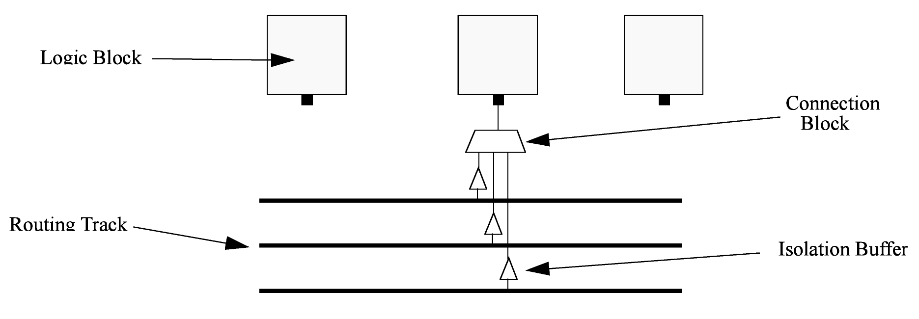
Fig. 21 Input Pin Diagram.
Required Attributes: - switch_name – Specifies the name of the
<switch>in the<switchlist>used to connect routing tracks to block input pins (i.e. the input connection block switch).
Required: Yes
- switch_name – Specifies the name of the
-
<area grid_logic_tile_area="float"/>" title="Permalink to this definition">¶ Required: Yes Specifies the default area used by each 1x1 grid logic tile (in MWTAs), excluding routing.
Used for an area estimate of the amount of area taken by all the functional blocks.
Note
This value can be overriden for specific
<pb_type>``s with the ``areaattribute.
-
<switch_block type="{wilton | subset | universal | custom}" fs="int"/>" title="Permalink to this definition">¶ Required Attributes: - type – The type of switch block to use.
- fs – The value of \(F_s\)
Required: Yes
This parameter controls the pattern of switches used to connect the (inter-cluster) routing segments. Three fairly simple patterns can be specified with a single keyword each, or more complex custom patterns can be specified.
Non-Custom Switch Blocks:
When using bidirectional segments, all the switch blocks have \(F_s\) = 3 [BFRV92]. That is, whenever horizontal and vertical channels intersect, each wire segment can connect to three other wire segments. The exact topology of which wire segment connects to which can be one of three choices. The subset switch box is the planar or domain-based switch box used in the Xilinx 4000 FPGAs – a wire segment in track 0 can only connect to other wire segments in track 0 and so on. The wilton switch box is described in [Wil97], while the universal switch box is described in [CWW96]. To see the topology of a switch box, simply hit the “Toggle RR” button when a completed routing is on screen in VPR. In general the wilton switch box is the best of these three topologies and leads to the most routable FPGAs.
When using unidirectional segments, one can specify an \(F_s\) that is any multiple of 3. We use a modified wilton switch block pattern regardless of the specified switch_block_type. For all segments that start/end at that switch block, we follow the wilton switch block pattern. For segments that pass through the switch block that can also turn there, we cannot use the wilton pattern because a unidirectional segment cannot be driven at an intermediate point, so we assign connections to starting segments following a round robin scheme (to balance mux size).
Note
The round robin scheme is not tileable.
Custom Switch Blocks:
Specifying
customallows custom switch blocks to be described under the<switchblocklist>XML node, the format for which is described in Custom Switch Blocks. If the switch block is specified ascustom, thefsfield does not have to be specified, and will be ignored if present.
-
<chan_width_distr>content</chan_width_distr>¶ Content inside this tag is only used when VPR is in global routing mode. The contents of this tag are described in Global Routing Information.
-
<default_fc in_type="{frac|abs}" in_val="{int|float}" out_type="{frac|abs}" out_val="{int|float}"/>" title="Permalink to this definition">¶ This defines the default Fc specification, if it is not specified within a
<fc>tag inside a top-level complex block. The attributes have the same meaning as the <fc> tag attributes.
Switches
The tags within the <switchlist> tag specifies the switches used to connect wires and pins together.
-
<switch type="{mux|tristate|pass_gate|short|buffer}" name="string" R="float" Cin="float" Cout="float" Tdel="float" buf_size="{auto|float}" mux_trans_size="float", power_buf_size="int"/>" title="Permalink to this definition">¶ Describes a switch in the routing architecture.
Example:
<switch type="mux" name="my_awsome_mux" R="551" Cin=".77e-15" Cout="4e-15" Tdel="58e-12" mux_trans_size="2.630740" buf_size="27.645901"/>
Required Attributes: - type –
The type of switch:
mux: An isolating, configurable multiplexertristate: An isolating, configurable tristate-able bufferpass_gate: A non-isolating, configurable pass gateshort: A non-isolating, non-configurable electrical short (e.g. between two segments).buffer: An isolating, non-configurable non-tristate-able buffer (e.g. in-line along a segment).
Isolation
Isolating switches include a buffer which partition their input and output into separate DC-connected sub-circuits. This helps reduce RC wire delays.
Non-isolating switch do not isolate their input and output, which can increase RC wire delays.
Configurablity
Configurable switches can be turned on/off at configuration time.
Non-configurable switches can not be controlled at configuration time. These are typically used to model non-optional connections such as electrical shorts and in-line buffers.
- name – A unique name identifying the switch
- R – Resistance of the switch.
- Cin – Input capacitance of the switch.
- Cout – Output capacitance of the switch.
Optional Attributes: - Tdel –
Intrinsic delay through the switch. If this switch was driven by a zero resistance source, and drove a zero capacitance load, its delay would be: \(T_{del} + R \cdot C_{out}\).
The ‘switch’ includes both the mux and buffer
muxtype switches.Note
Required if no
<Tdel>tags are specifiedNote
A
<switch>’s resistance (R) and output capacitance (Cout) have no effect on delay when used for the input connection block, since VPR does not model the resistance/capacitance of block internal wires. - buf_size –
Specifies the buffer size in minimum-width transistor area (:term`MWTA`) units.
If set to
auto, sized automatically from the R value. This allows you to use timing models without R’s and C’s and still be able to measure area.Note
Required for all isolating switch types.
Default:
auto - mux_trans_size –
Specifies the size (in minimum width transistors) of each transistor in the two-level mux used by
muxtype switches.Note
Valid only for
muxtype switches. - power_buf_size – Used for power estimation. The size is the drive strength of the buffer, relative to a minimum-sized inverter.
-
<Tdel num_inputs="int" delay="float"/>" title="Permalink to this definition">¶ Instead of specifying a single Tdel value, a list of Tdel values may be specified for different values of switch fan-in. Delay is linearly extrapolated/interpolated for any unspecified fanins based on the two closest fanins.
Required Attributes: - num_inputs – The number of switch inputs (fan-in)
- delay – The intrinsic switch delay when the switch topology has the specified number of switch inputs
Example:
<switch type="mux" name="my_mux" R="522" Cin="3.1e-15" Cout="3e-15" mux_trans_size="1.7" buf_size="23">
    <Tdel num_inputs="12" delay="8.00e-11"/>
    <Tdel num_inputs="15" delay="8.4e-11"/>
    <Tdel num_inputs="20" delay="9.4e-11"/>
</switch>
- type –
Global Routing Information
If global routing is to be performed, channels in different directions and in different parts of the FPGA can be set to different relative widths.
This is specified in the content within the <chan_width_distr> tag.
Note
If detailed routing is to be performed, all the channels in the FPGA must have the same width.
-
<x distr="{gaussian|uniform|pulse|delta}" peak="float" width=" float" xpeak=" float" dc=" float"/>" title="Permalink to this definition">¶ Required Attributes: - distr – The channel width distribution function
- peak – The peak value of the distribution
Optional Attributes: - width – The width of the distribution. Required for
pulseandgaussian. - xpeak – Peak location horizontally. Required for
pulse,gaussiananddelta. - dc – The DC level of the distribution. Required for
pulse,gaussiananddelta.
Sets the distribution of tracks for the x-directed channels – the channels that run horizontally.
Most values are from 0 to 1.
If uniform is specified, you simply specify one argument, peak. This value (by convention between 0 and 1) sets the width of the x-directed core channels relative to the y-directed channels and the channels between the pads and core. Fig. 22 should clarify the specification of uniform (dashed line) and pulse (solid line) channel widths. The gaussian keyword takes the same four parameters as the pulse keyword, and they are all interpreted in exactly the same manner except that in the gaussian case width is the standard deviation of the function.
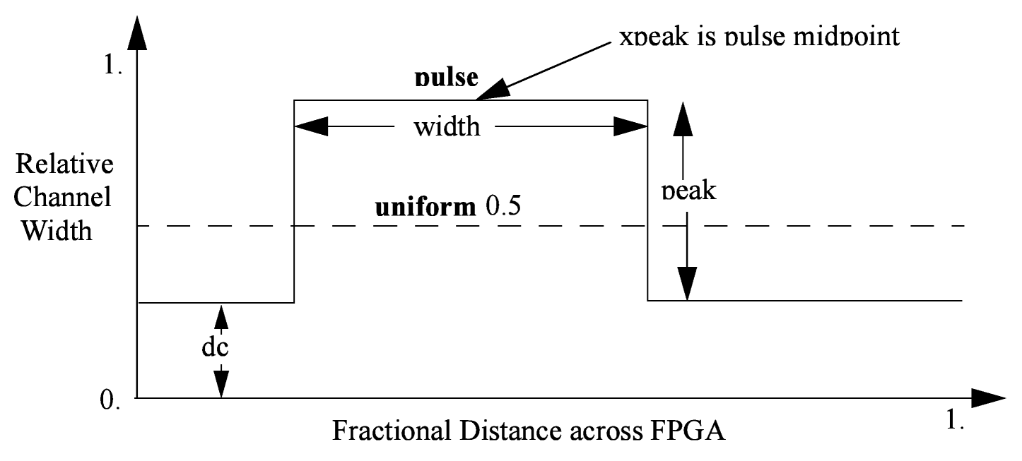
Fig. 22 Channel Distribution
The delta function is used to specify a channel width distribution in which all the channels have the same width except one. The syntax is chan_width_x delta peak xpeak dc. Peak is the extra width of the single wide channel. Xpeak is between 0 and 1 and specifies the location within the FPGA of the extra-wide channel – it is the fractional distance across the FPGA at which this extra-wide channel lies. Finally, dc specifies the width of all the other channels. For example, the statement chan_width_x delta 3 0.5 1 specifies that the horizontal channel in the middle of the FPGA is four times as wide as the other channels.
Examples:
<x distr="uniform" peak="1"/>
<x distr="gaussian" width="0.5" peak="0.8" xpeak="0.6" dc="0.2"/>
Complex Blocks
See also
For a step-by-step walkthrough on building a complex block see Architecture Modeling.
The content within the <complexblocklist> describes the complex blocks found within the FPGA.
Each type of complex block is specified with a top-level <pb_type> tag within the <complexblocklist> tag.
PB Type
-
<pb_type name="string" num_pb="int" blif_model="string" capacity="int" width="int" height="int" area="float" class="{lut|filpflop|memory}"/>" title="Permalink to this definition">¶ Specifies a top-level complex block, or a complex block’s internal components (sub-blocks). Which attributes are applicable depends on where the
<pb_type>tag falls within the hierarchy:- Top Level: A child of the
<complexblocklist> - Intermediate: A child of another
<pb_type> - Primitive/Leaf: Contains no
<pb_type>children
For example:
<complexblocklist>
    <pb_type name="CLB"/> <!-- Top level -->
        ...
        <pb_type name="ble"/> <!-- Intermediate -->
            ...
            <pb_type name="lut"/> <!-- Primitive -->
                ...
            </pb_type>
            <pb_type name="ff"/> <!-- Primitive -->
                ...
            </pb_type>
            ...
        </pb_type>
        ...
    </pb_type>
    ...
</complexblocklist>
General:
Required Attributes: - name –
The name of this pb_type.
The name must be unique with respect to any parent, sibling, or child
<pb_type>.
Top Level Only:
Optional Attributes: - capacity –
The number of instances of this block type at each grid location
Default:
1For example:
<pb_type name="IO" capacity="2"/>
    ...
</pb_type>
specifies there are two instances of the block type
IOat each of its grid locations. - width –
The width of the block type in grid tiles
Default:
1 - height –
The height of the block type in grid tiles
Default:
1 - area –
The logic area (in MWTA) of the block type
Default: from the
<area>tag
Intermediate or Primitive:
Optional Attributes: - num_pb –
The number of instances of this pb_type at the current hierarchy level.
Default:
1For example:
<pb_type name="CLB">
    ...
    <pb_type name="ble" num_pb="10"/>
       ...
    </pb_type>
    ...
</pb_type>
would specify that the pb_type
CLBcontains 10 instances of theblepb_type.
Primitive Only:
Required Attributes: - blif_model –
Specifies the netlist primitive which can be implemented by this pb_type.
Accepted values:
.input: A BLIF netlist input.output: A BLIF netlist output.names: A BLIF .names (LUT) primitive.latch: A BLIF .latch (DFF) primitive.subckt <custom_type>: A user defined black-box primitive.
For example:
<pb_type name="my_adder" blif_model=".subckt adder"/>
   ...
</pb_type>
would specify that the pb_type
my_addercan implement a black-box BLIF primitive namedadder.Note
The input/output/clock ports for primitive pb_types must match the ports specified in the
<models>section.
Optional Attributes: - class –
Specifies that this primitive is of a specialized type which should be treated specially.
See also
Classes for more details.
- Top Level: A child of the
The following tags are common to all <pb_type> tags:
-
<input name="string" num_pins="int" equivalent="{none|full}" is_non_clock_global="{true|false}"/>" title="Permalink to this definition">¶ Defines an input port. Multple input ports are described using multiple
<input>tags.Required Attributes: - name – Name of the input port.
- num_pins – Number of pins the input port has.
Optional Attributes: - equivalent –
Note
Applies only to top-level pb_type.
Describes if the pins of the port are logically equivalent. Input logical equivalence means that the pin order can be swapped without changing functionality. For example, an AND gate has logically equivalent inputs because you can swap the order of the inputs and it’s still correct; an adder, on the otherhand, is not logically equivalent because if you swap the MSB with the LSB, the results are completely wrong. LUTs are also considered logically equivalent since the logic function (LUT mask) can be rotated to account for pin swapping.
none: No input pins are logically equivalent.Input pins can not be swapped by the router. (Generates a unique SINK rr-node for each block input port pin.)full: All input pins are considered logically equivalent (e.g. due to logical equivalance or a full-crossbar within the cluster).All input pins can be swapped without limitation by the router. (Generates a single SINK rr-node shared by each input port pin.)
default:
none - is_non_clock_global –
Note
Applies only to top-level pb_type.
Describes if this input pin is a global signal that is not a clock. Very useful for signals such as FPGA-wide asynchronous resets. These signals have their own dedicated routing channels and so should not use the general interconnect fabric on the FPGA.
-
<output name="string" num_pins="int" equivalent="{none|full|instance}"/>" title="Permalink to this definition">¶ Defines an output port. Multple output ports are described using multiple
<output>tagsRequired Attributes: - name – Name of the output port.
- num_pins – Number of pins the output port has.
Optional Attributes: - equivalent –
Note
Applies only to top-level pb_type.
Describes if the pins of the output port are logically equivalent:
none: No output pins are logically equivalent.Output pins can not be swapped by the router. (Generates a unique SRC rr-node for each block output port pin.)full: All output pins are considered logically equivalent.All output pins can be swapped without limitation by the router. For example, this option would be appropriate to model an output port which has a full crossbar between it and the logic within the block that drives it. (Generates a single SRC rr-node shared by each output port pin.)instance: Models that sub-instances within a block (e.g. LUTs/BLEs) can be swapped to achieve a limited form of output pin logical equivalence.Likefull, this generates a single SRC rr-node shared by each output port pin. However, each net originating from this source can use only one output pin from the equivalence group. This can be useful in modeling more complex forms of equivalence in which you can swap which BLE implements which function to gain access to different inputs.Warning
When using
instanceequivalence you must be careful to ensure output swapping would not make the cluster internal routing (previously computed by the clusterer) illegal; the tool does not update the cluster internal routing due to output pin swapping.
Default:
none
-
<clock name="string" num_pins="int" equivalent="{none|full}"/>" title="Permalink to this definition">¶ Describes a clock port. Multple clock ports are described using multiple
<clock>tags. See above descriptions on inputs
-
<mode name="string">" title="Permalink to this definition">¶ Required Attributes: - name – Name for this mode. Must be unique compared to other modes.
Specifies a mode of operation for the
<pb_type>. Each child mode tag denotes a different mode of operation for the<pb_type>. Each mode tag may contains other<pb_type>and<interconnect>tags.Note
Modes within the same parent
<pb_type>are mutually exclusive.Note
If a
<pb_type>has only one mode of operation the mode tag can be omitted.For example:
<!--A fracturable 6-input LUT-->
<pb_type name="lut">
    ...
    <mode name="lut6">
        <!--Can be used as a single 6-LUT-->
        <pb_type name="lut6" num_pb="1">
            ...
        </pb_type>
        ...
    </mode>
    ...
    <mode name="lut5x2">
        <!--Or as two 5-LUTs-->
        <pb_type name="lut5" num_pb="2">
            ...
        </pb_type>
        ...
    </mode>
</pb_type>
specifies the
lutpb_type can be used as either a single 6-input LUT, or as two 5-input LUTs (but not both).
The following tags are unique to the top level <pb_type> of a complex logic block. They describe how a complex block interfaces with the inter-block world.
-
<fc in_type="{frac|abs}" in_val="{int|float}" out_type="{frac|abs}" out_val="{int|float}">" title="Permalink to this definition">¶ Required Attributes: - in_type –
Indicates how the \(F_c\) values for input pins should be interpreted.
frac: The fraction of tracks of each wire/segment type.abs: The absolute number of tracks of each wire/segment type. - in_val – Fraction or absolute number of tracks to which each input pin is connected.
- out_type –
Indicates how the \(F_c\) values for output pins should be interpreted.
frac: The fraction of tracks of each wire/segment type.abs: The absolute number of tracks of each wire/segment type. - out_val – Fraction or absolute number of wires/segments to which each output pin connects.
Sets the number of tracks/wires to which each logic block pin connects in each channel bordering the pin.
The \(F_c\) value [BFRV92] is interpreted as applying to each wire/segment type individually (see example).
When generating the FPGA routing architecture VPR will try to make ‘good’ choices about how pins and wires interconnect; for more details on the criteria and methods used see [BR00].
Note
If
<fc>is not specified for a complex block, the architecture’s<default_fc>is used.Note
For unidirection routing architectures absolute \(F_c\) values must be a multiple of 2.
Example:
Consider a routing architecture with 200 length 4 (L4) wires and 50 length 16 (L16) wires per channel, and the following Fc specification:
<fc in_type="frac" in_val="0.1" out_type="abs" out_val="25">
The above specifies that each:
- input pin connects to 20 L4 tracks (10% of the 200 L4s) and 5 L16 tracks (10% of the 50 L16s), and
- output pin connects to 25 L4 tracks and 25 L16 tracks.
Overriding Values:
-
<fc_override fc_type="{frac|abs}" fc_val="{int|float}", port_name="{string}" segment_name="{string}">" title="Permalink to this definition">¶ Allows \(F_c\) values to be overriden on a port or wire/segment type basis.
Required Attributes: - fc_type –
Indicates how the override \(F_c\) value should be interpreted.
frac: The fraction of tracks of each wire/segment type.abs: The absolute number of tracks of each wire/segment type. - fc_val – Fraction or absolute number of tracks in a channel.
Optional Attributes: - port_name – The name of the port to which this override applies. If left unspecified this override applies to all ports.
- segment_name – The name of the segment (defined under
<segmentlist>) to which this override applies. If left unspecified this override applies to all segments.
Note
At least one of
port_nameorsegment_namemust be specified.Port Override Example: Carry Chains
If you have complex block pins that do not connect to general interconnect (eg. carry chains), you would use the
<fc_override>tag, within the<fc>tag, to specify them:<fc_override fc_type="frac" fc_val="0" port_name="cin"/> <fc_override fc_type="frac" fc_val="0" port_name="cout"/>
Where the attribute
port_nameis the name of the pin (cinandcoutin this example).Segment Override Example:
It is also possible to specify per
<segment>(i.e. routing wire) overrides:<fc_override fc_type="frac" fc_val="0.1" segment_name="L4"/>
Where the above would cause all pins (both inputs and outputs) to use a fractional \(F_c\) of
0.1when connecting to segments of typeL4.Combined Port and Segment Override Example:
The
port_nameandsegment_nameattributes can be used together. For example:<fc_override fc_type="frac" fc_val="0.1" port_name="my_input" segment_name="L4"/> <fc_override fc_type="frac" fc_val="0.2" port_name="my_output" segment_name="L4"/>
specifies that port
my_inputuse a fractional \(F_c\) of0.1when connecting to segments of typeL4, while the portmy_outputuses a fractional \(F_c\) of0.2when connecting to segments of typeL4. All other port/segment combinations would use the default \(F_c\) values.- fc_type –
- in_type –
-
<pinlocations pattern="{spread|perimeter|custom}">" title="Permalink to this definition">¶ Required Attributes: - pattern –
spreaddenotes that the pins are to be spread evenly on all sides of the complex block.Note
Includes internal sides of blocks with width > 1 and/or height > 1.
perimeterdenotes that the pins are to be spread evenly on perimeter sides of the complex block.Note
Excludes the internal sides of blocks with width > 1 and/or height > 1.
spread_inputs_perimeter_outputsdenotes that inputs pins are to be spread on all sides of the complex block, but output pins are to be spread only on perimeter sides of the block.Note
This is useful for ensuring outputs do not connect to wires which fly-over a width > 1 and height > 1 block (e.g. if using
shortorbufferconnections instead of a fully configurable switch block within the block).customallows the architect to specify specifically where the pins are to be placed using<loc>tags.
Describes the locations where the input, output, and clock pins are distributed in a complex logic block.
-
<loc side="{left|right|bottom|top}" xoffset="int" yoffset="int">name_of_complex_logic_block.port_name[int:int] ... </loc>name_of_complex_logic_block.port_name[int:int]..." title="Permalink to this definition">¶ Note
...represents repeat as needed. Do not put...in the architecture file.Required Attributes: - side – Specifies which of the four sides of a grid location the pins in the contents are located.
Optional Attributes: - xoffset –
Specifies the horizontal offset (in grid units) from block origin (bottom left corner). The offset value must be less than the width of the block.
Default:
0 - yoffset –
Specifies the vertical offset (in grid units) from block origin (bottom left corner). The offset value must be less than the height of the block.
Default:
0
Physical equivalence for a pin is specified by listing a pin more than once for different locations. For example, a LUT whose output can exit from the top and bottom of a block will have its output pin specified twice: once for the top and once for the bottom.
Note
If the
<pinlocations>tag is missing, aspreadpattern is assumed.- pattern –
-
<switchblock_locations pattern="{external_full_internal_straight|all|external|internal|none|custom}" internal_switch="string">" title="Permalink to this definition">¶ Describes where global routing switchblocks are created in relation to the complex block.
Note
If the
<switchblock_locations>tag is left unspecified the default pattern is assumed.Optional Attributes: - pattern –
external_full_internal_straight: creates full switchblocks outside and straight switchblocks inside the complex blockall: creates switchblocks wherever routing channels crossexternal: creates switchblocks wherever routing channels cross outside the complex blockinternal: creates switchblocks wherever routing channels cross inside the complex blocknone: denotes that no switchblocks are created for the complex blockcustom: allows the architect to specify custom switchblock locations and types using<sb_loc>tags
Default:
external_full_internal_straight

Fig. 23 Switchblock Location Patterns for a width = 2, height = 3 complex block
Optional Attributes: - internal_switch –
The name of a switch (from
<switchlist>) which should be used for internal switch blocks.Default: The default switch for the wire
<segment>Note
This is typically used to specify that internal wire segments are electrically shorted together using a
shorttype<switch>.
Example: Electrically Shorted Internal Straight Connections
In some architectures there are no switch blocks located ‘within’ a block, and the wires crossing over the block are instead electrcially shorted to their ‘straight-through’ connections.
To model this we first define a special
shorttype switch to electrically short such segments together:<switchlist> <switch type="short" name="electrical_short" R="0" Cin="0" Tdel="0"/> </switchlist>
Next, we use the pre-defined
external_full_internal_straightpattern, and that such connections should use ourelectrical_shortswitch.<switchblock_locations pattern="external_full_internal_straight" internal_switch="electrical_short"/>
-
<sb_loc type="{full|straight|turns|none}" xoffset="int" yoffset="int", switch_override="string">" title="Permalink to this definition">¶ Specifies the type of switchblock to create at a particular location relative to a complex block for the
customswitchblock location pattern.Required Attributes: - type –
Specifies the type of switchblock to be created at this location:
full: denotes that a full switchblock will be created (i.e. bothstaightandturns)straight: denotes that a switchblock with only straight-through connections will be created (i.e. noturns)turns: denotes that a switchblock with only turning connections will be created (i.e. nostraight)none: denotes that no switchblock will be created
Default:
full
Fig. 24 Switchblock Types
Optional Attributes: - xoffset –
Specifies the horizontal offset (in grid units) from block origin (bottom left corner). The offset value must be less than the width of the block.
Default:
0 - yoffset –
Specifies the vertical offset (in grid units) from block origin (bottom left corner). The offset value must be less than the height of the block.
Default:
0 - switch_override –
The name of a switch (from
<switchlist>) which should be used to construct the switch block at this location.Default: The default switch for the wire
<segment>
Note
The switchblock associated with a grid tile is located to the top-right of the grid tile
Example: Custom Description of Electrically Shorted Internal Straight Connections
If we assume a width=2, height=3 block (e.g. Fig. 23), we can use a custom pattern to specify an architecture equivalent to the ‘Electrically Shorted Internal Straight Connections’ example:
<switchblock_locations pattern="custom">
    <!-- Internal: using straight electrical shorts -->
    <sb_loc type="straight" xoffset="0" yoffset="0" switch_override="electrical_short">
    <sb_loc type="straight" xoffset="0" yoffset="1" switch_override="electrical_short">

    <!-- External: using default switches -->
    <sb_loc type="full" xoffset="0" yoffset="2"> <!-- Top edge -->
    <sb_loc type="full" xoffset="1" yoffset="0"> <!-- Right edge -->
    <sb_loc type="full" xoffset="1" yoffset="1"> <!-- Right edge -->
    <sb_loc type="full" xoffset="1" yoffset="2"> <!-- Top Right -->
<switchblock_locations/>
- type –
- pattern –
Interconnect
As mentioned earlier, the mode tag contains <pb_type> tags and an <interconnect> tag.
The following describes the tags that are accepted in the <interconnect> tag.
-
<complete name="string" input="string" output="string"/>" title="Permalink to this definition">¶ Required Attributes: - name – Identifier for the interconnect.
- input – Pins that are inputs to this interconnect.
- output – Pins that are outputs of this interconnect.
Describes a fully connected crossbar. Any pin in the inputs can connect to any pin at the output.
Example:
<complete input="Top.in" output="Child.in"/>
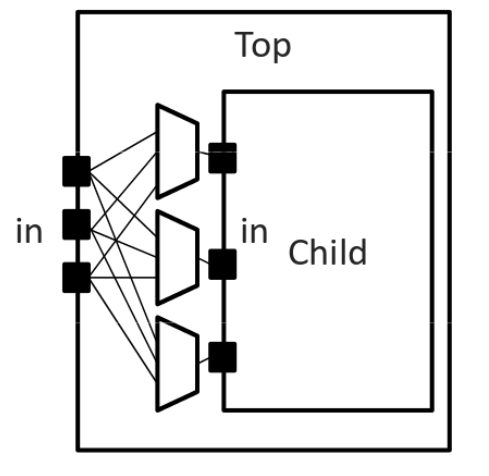
Fig. 25 Complete interconnect example.
-
<direct name="string" input="string" output="string"/>" title="Permalink to this definition">¶ Required Attributes: - name – Identifier for the interconnect.
- input – Pins that are inputs to this interconnect.
- output – Pins that are outputs of this interconnect.
Describes a 1-to-1 mapping between input pins and output pins.
Example:
<direct input="Top.in[2:1]" output="Child[1].in"/>

Fig. 26 Direct interconnect example.
-
<mux name="string" input="string" output="string"/>" title="Permalink to this definition">¶ Required Attributes: - name – Identifier for the interconnect.
- input – Pins that are inputs to this interconnect. Different data lines are separated by a space.
- output – Pins that are outputs of this interconnect.
Describes a bus-based multiplexer.
Note
Buses are not yet supported so all muxes must use one bit wide data only!
Example:
<mux input="Top.A Top.B" output="Child.in"/>

Fig. 27 Mux interconnect example.
A <complete>, <direct>, or <mux> tag may take an additional, optional, tag called <pack_pattern> that is used to describe molecules.
A pack pattern is a power user feature directing that the CAD tool should group certain netlist atoms (eg. LUTs, FFs, carry chains) together during the CAD flow.
This allows the architect to help the CAD tool recognize structures that have limited flexibility so that netlist atoms that fit those structures be kept together as though they are one unit.
This tag impacts the CAD tool only, there is no architectural impact from defining molecules.
-
<pack_pattern name="string" in_port="string" out_port="string"/>" title="Permalink to this definition">¶ Warning
This is a power user option. Unless you know why you need it, you probably shouldn’t specify it.
Required Attributes: - name – The name of the pattern.
- in_port – The input pins of the edges for this pattern.
- out_port – Which output pins of the edges for this pattern.
This tag gives a hint to the CAD tool that certain architectural structures should stay together during packing. The tag labels interconnect edges with a pack pattern name. All primitives connected by the same pack pattern name becomes a single pack pattern. Any group of atoms in the user netlist that matches a pack pattern are grouped together by VPR to form a molecule. Molecules are kept together as one unit in VPR. This is useful because it allows the architect to help the CAD tool assign atoms to complex logic blocks that have interconnect with very limited flexibility. Examples of architectural structures where pack patterns are appropriate include: optionally registered inputs/outputs, carry chains, multiply-add blocks, etc.
There is a priority order when VPR groups molecules. Pack patterns with more primitives take priority over pack patterns with less primitives. In the event that the number of primitives is the same, the pack pattern with less inputs takes priority over pack patterns with more inputs.
Special Case:
To specify carry chains, we use a special case of a pack pattern. If a pack pattern has exactly one connection to a logic block input pin and exactly one connection to a logic block output pin, then that pack pattern takes on special properties. The prepacker will assume that this pack pattern represents a structure that spans multiple logic blocks using the logic block input/output pins as connection points. For example, lets assume that a logic block has two, 1-bit adders with a carry chain that links adjacent logic blocks. The architect would specify those two adders as a pack pattern with links to the logic block cin and cout pins. Lets assume the netlist has a group of 1-bit adder atoms chained together to form a 5-bit adder. VPR will break that 5-bit adder into 3 molecules: two 2-bit adders and one 1-bit adder connected in order by a the carry links.
Example:
Consider a classic basic logic element (BLE) that consists of a LUT with an optionally registered flip-flop. If a LUT is followed by a flip-flop in the netlist, the architect would want the flip-flop to be packed with the LUT in the same BLE in VPR. To give VPR a hint that these blocks should be connected together, the architect would label the interconnect connecting the LUT and flip-flop pair as a pack_pattern:
<pack_pattern name="ble" in_port="lut.out" out_port="ff.D"/>
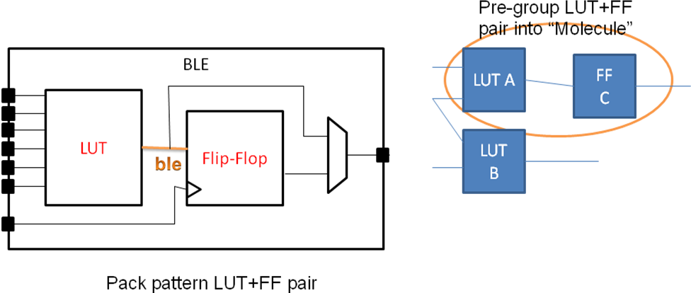
Fig. 28 Pack Pattern Example.
Classes
Using these structures, we believe that one can describe any digital complex logic block.
However, we believe that certain kinds of logic structures are common enough in FPGAs that special shortcuts should be available to make their specification easier.
These logic structures are: flip-flops, LUTs, and memories.
These structures are described using a class=string attribute in the <pb_type> primitive.
The classes we offer are:
-
class="lut"¶ Describes a K-input lookup table.
The unique characteristic of a lookup table is that all inputs to the lookup table are logically equivalent. When this class is used, the input port must have a
port_class="lut_in"attribute and the output port must have aport_class="lut_out"attribute.
-
class="flipflop"¶ Describes a flipflop.
Input port must have a
port_class="D"attribute added. Output port must have aport_class="Q"attribute added. Clock port must have aport_class="clock"attribute added.
-
class="memory"¶ Describes a memory.
Memories are unique in that a single memory physical primitive can hold multiple, smaller, logical memories as long as:
- The address, clock, and control inputs are identical and
- There exists sufficient physical data pins to satisfy the netlist memories when the different netlist memories are merged together into one physical memory.
Different types of memories require different attributes.
Single Port Memories Require:
- An input port with
port_class="address"attribute - An input port with
port_class="data_in"attribute - An input port with
port_class="write_en"attribute - An output port with
port_class="data_out"attribute - A clock port with
port_class="clock"attribute
Dual Port Memories Require:
- An input port with
port_class="address1"attribute - An input port with
port_class="data_in1"attribute - An input port with
port_class="write_en1"attribute - An input port with
port_class="address2"attribute - An input port with
port_class="data_in2"attribute - An input port with
port_class="write_en2"attribute - An output port with
port_class="data_out1"attribute - An output port with
port_class="data_out2"attribute - A clock port with
port_class="clock"attribute
Timing
See also
For examples of primitive timing modeling specifications see the Primitive Block Timing Modeling Tutorial
Timing is specified through tags contained with in pb_type, complete, direct, or mux tags as follows:
-
<delay_constant max="float" min="float" in_port="string" out_port="string"/>" title="Permalink to this definition">¶ Optional Attributes: - max – The maximum delay value.
- min – The minimum delay value.
Required Attributes: - in_port – The input port name.
- out_port – The output port name.
Specifies a maximum and/or minimum delay from in_port to out_port.
- If
in_portandout_portare non-sequential (i.e combinational) inputs specifies the combinational path delay between them. - If
in_portandout_portare sequential (i.e. haveT_setupand/orT_clock_to_Qtags) specifies the combinational delay between the primitive’s input and/or output registers.
Note
At least one of the
maxorminattributes must be specifiedNote
If only one of
maxorminare specified the unspecified value is implicitly set to the same value
-
<delay_matrix type="{max | min}" in_port="string" out_port="string"> matrix </delay>matrix" title="Permalink to this definition">¶ Required Attributes: - type – Specifies the delay type.
- in_port – The input port name.
- out_port – The output port name.
- matrix – The delay matrix.
Describe a timing matrix for all edges going from
in_porttoout_port. Number of rows of matrix should equal the number of inputs, number of columns should equal the number of outputs.- If
in_portandout_portare non-sequential (i.e combinational) inputs specifies the combinational path delay between them. - If
in_portandout_portare sequential (i.e. haveT_setupand/orT_clock_to_Qtags) specifies the combinational delay between the primitive’s input and/or output registers.
Example: The following defines a delay matrix for a 4-bit input port
in, and 3-bit output portout:<delay_matrix type="max" in_port="in" out_port="out"> 1.2e-10 1.4e-10 3.2e-10 4.6e-10 1.9e-10 2.2e-10 4.5e-10 6.7e-10 3.5e-10 7.1e-10 2.9e-10 8.7e-10 </delay>
Note
To specify both
maxandmindelays two<delay_matrix>should be used.
-
<T_setup value="float" port="string" clock="string"/>" title="Permalink to this definition">¶ Required Attributes: - value – The setup time value.
- port – The port name the setup constraint applies to.
- clock – The port name of the clock the setup constraint is specified relative to.
Specifies a port’s setup constraint.
- If
portis an input specifies the external setup time of the primitive’s input register (i.e. for paths terminating at the input register). - If
portis an output specifies the internal setup time of the primitive’s output register (i.e. for paths terminating at the output register) .
Note
Applies only to primitive
<pb_type>tags
-
<T_hold value="float" port="string" clock="string"/>" title="Permalink to this definition">¶ Required Attributes: - value – The hold time value.
- port – The port name the setup constraint applies to.
- clock – The port name of the clock the setup constraint is specified relative to.
Specifies a port’s hold constraint.
- If
portis an input specifies the external hold time of the primitive’s input register (i.e. for paths terminating at the input register). - If
portis an output specifies the internal hold time of the primitive’s output register (i.e. for paths terminating at the output register) .
Note
Applies only to primitive
<pb_type>tags
-
<T_clock_to_Q max="float" min="float" port="string" clock="string"/>" title="Permalink to this definition">¶ Optional Attributes: - max – The maximum clock-to-Q delay value.
- min – The minimum clock-to-Q delay value.
Required Attributes: - port – The port name the delay value applies to.
- clock – The port name of the clock the clock-to-Q delay is specified relative to.
Specifies a port’s clock-to-Q delay.
- If
portis an input specifies the internal clock-to-Q delay of the primitive’s input register (i.e. for paths starting at the input register). - If
portis an output specifies the external clock-to-Q delay of the primitive’s output register (i.e. for paths starting at the output register) .
Note
At least one of the
maxorminattributes must be specifiedNote
If only one of
maxorminare specified the unspecified value is implicitly set to the same valueNote
Applies only to primitive
<pb_type>tags
Modeling Sequential Primitive Internal Timing Paths
See also
For examples of primitive timing modeling specifications see the Primitive Block Timing Modeling Tutorial
By default, if only <T_setup> and <T_clock_to_Q> are specified on a primitive pb_type no internal timing paths are modeled.
However, such paths can be modeled by using <delay_constant> and/or <delay_matrix> can be used in conjunction with <T_setup> and <T_clock_to_Q>.
This is useful for modeling the speed-limiting path of an FPGA hard block like a RAM or DSP.
As an example, consider a sequential black-box primitive named seq_foo which has an input port in, output port out, and clock clk:
<pb_type name="seq_foo" blif_model=".subckt seq_foo" num_pb="1">
    <input name="in" num_pins="4"/>
    <output name="out" num_pins="1"/>
    <clock name="clk" num_pins="1"/>

    <!-- external -->
    <T_setup value="80e-12" port="seq_foo.in" clock="clk"/>
    <T_clock_to_Q max="20e-12" port="seq_foo.out" clock="clk"/>

    <!-- internal -->
    <T_clock_to_Q max="10e-12" port="seq_foo.in" clock="clk"/>
    <delay_constant max="0.9e-9" in_port="seq_foo.in" out_port="seq_foo.out"/>
    <T_setup value="90e-12" port="seq_foo.out" clock="clk"/>
</pb_type>
To model an internal critical path delay, we specify the internal clock-to-Q delay of the input register (10ps), the internal combinational delay (0.9ns) and the output register’s setup time (90ps). The sum of these delays corresponds to a 1ns critical path delay.
Note
Primitive timing paths with only one stage of registers can be modeled by specifying <T_setup> and <T_clock_to_Q> on only one of the ports.
Power
See also
Power Estimation, for the complete list of options, their descriptions, and required sub-fields.
-
<power method="string">contents</power>contents" title="Permalink to this definition">¶ Optional Attributes: - method –
Indicates the method of power estimation used for the given pb_type.
Must be one of:
specify-sizeauto-sizepin-toggleC-internalabsoluteignoresum-of-children
Default:
auto-size.See also
Power Architecture Modelling for a detailed description of the various power estimation methods.
The
contentsof the tag can consist of the following tags:<dynamic_power><static_power><pin>
- method –
-
<dynamic_power power_per_instance="float" C_internal="float"/>" title="Permalink to this definition">¶ Optional Attributes: - power_per_instance – Absolute power in Watts.
- C_internal – Block capacitance in Farads.
-
<static_power power_per_instance="float"/>" title="Permalink to this definition">¶ Optional Attributes: - power_per_instance – Absolute power in Watts.
-
<port name="string" energy_per_toggle="float" scaled_by_static_prob="string" scaled_by_static_prob_n="string"/>" title="Permalink to this definition">¶ Required Attributes: - name – Name of the port.
- energy_per_toggle – Energy consumed by a toggle on the port specified in
name.
Optional Attributes: - scaled_by_static_prob – Port name by which to scale
energy_per_togglebased on its logic high probability. - scaled_by_static_prob_n – Port name by which to scale
energy_per_togglebased on its logic low probability.
Wire Segments
The content within the <segmentlist> tag consists of a group of <segment> tags.
The <segment> tag and its contents are described below.
-
<segment name="unique_name" length="int" type="{bidir|unidir}" freq="float" Rmetal="float" Cmetal="float">content</segment>content" title="Permalink to this definition">¶ Required Attributes: - name – A unique alphanumeric name to identify this segment type.
- length –
Either the number of logic blocks spanned by each segment, or the keyword
longline. Longline means segments of this type span the entire FPGA array.Note
longlineis only supported on withbidirrouting - freq – The supply of routing tracks composed of this type of segment. VPR automatically determines the percentage of tracks for each segment type by taking the frequency for the type specified and dividing with the sum of all frequencies. It is recommended that the sum of all segment frequencies be in the range 1 to 100.
- Rmetal – Resistance per unit length (in terms of logic blocks) of this wiring track, in Ohms. For example, a segment of length 5 with Rmetal = 10 Ohms / logic block would have an end-to-end resistance of 50 Ohms.
- Cmetal – Capacitance per unit length (in terms of logic blocks) of this wiring track, in Farads. For example, a segment of length 5 with Cmetal = 2e-14 F / logic block would have a total metal capacitance of 10e-13F.
- directionality – This is either unidirectional or bidirectional and indicates whether a segment has multiple drive points (bidirectional), or a single driver at one end of the wire segment (unidirectional). All segments must have the same directionality value. See [LLTY04] for a description of unidirectional single-driver wire segments.
- content – The switch names and the depopulation pattern as described below.
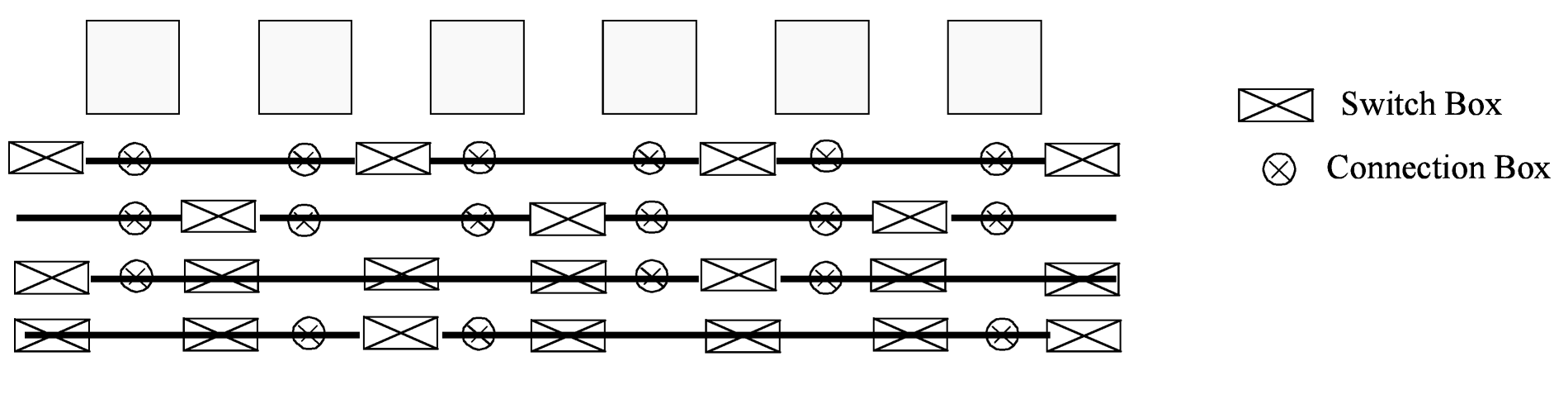
Fig. 29 Switch block and connection block pattern example with four tracks per channel
-
<sb type="pattern">int list</sb>intlist" title="Permalink to this definition">¶ This tag describes the switch block depopulation (as illustrated in Fig. 29) for this particular wire segment. For example, the first length 6 wire in the figure below has an sb pattern of
1 0 1 0 1 0 1. The second wire has a pattern of0 1 0 1 0 1 0. A1indicates the existence of a switch block and a0indicates that there is no switch box at that point. Note that there a 7 entries in the integer list for a length 6 wire. For a length L wire there must be L+1 entries separated by spaces.Note
Can not be specified for
longlinesegments (which assume full switch block population)
-
<cb type="pattern">int list</cb>intlist" title="Permalink to this definition">¶ This tag describes the connection block depopulation (as illustrated by the circles in Fig. 29) for this particular wire segment. For example, the first length 6 wire in the figure below has an sb pattern of
1 1 1 1 1 1. The third wire has a pattern of1 0 0 1 1 0. A1indicates the existence of a connection block and a0indicates that there is no connection box at that point. Note that there a 6 entries in the integer list for a length 6 wire. For a length L wire there must be L entries separated by spaces.Note
Can not be specified for
longlinesegments (which assume full connection block population)
-
<mux name="string"/>" title="Permalink to this definition">¶ Required Attributes: - name – Name of the mux switch type used to drive this type of segment.
Note
For UNIDIRECTIONAL only.
Tag must be included and
namemust be the same as the name you give in<switch type="mux" name="...
-
<wire_switch name="string"/>" title="Permalink to this definition">¶ Required Attributes: - name – Name of the switch type used by other wires to drive this type of segment.
Note
For BIDIRECTIONAL only.
Tag must be included and the name must be the same as the name you give in
<switch type="tristate|pass_gate" name="...for the switch which represents the wire switch in your architecture.
-
<opin_switch name="string"/>" title="Permalink to this definition">¶ Note
For BIDIRECTIONAL only.
Required Attributes: - name – Name of the switch type used by block pins to drive this type of segment.
Tag must be included and
namemust be the same as the name you give in<switch type="tristate|pass_gate" name="...for the switch which represents the output pin switch in your architecture.Note
In unidirectional segment mode, there is only a single buffer on the segment. Its type is specified by assigning the same switch index to both wire_switch and opin_switch. VPR will error out if these two are not the same.
Note
The switch used in unidirectional segment mode must be buffered.
Clocks
The clocking configuration is specified with <clock> tags within the <clocks> section.
Note
Currently the information in the <clocks> section is only used for power estimation.
See also
Power Estimation for more details.
-
<clock C_wire="float" C_wire_per_m="float" buffer_size={"float"|"auto"}/>" title="Permalink to this definition">¶ Optional Attributes: - C_wire – The absolute capacitance, in Farads, of the wire between each clock buffer.
- C_wire_per_m – The wire capacitance, in Farads per Meter.
- buffer_size – The size of each clock buffer.
Power
Additional power options are specified within the <architecture> level <power> section.
See also
See Power Estimation for full documentation on how to perform power estimation.
Direct Inter-block Connections
The content within the <directlist> tag consists of a group of <direct> tags.
The <direct> tag and its contents are described below.
-
<direct name="string" from_pin="string" to_pin="string" x_offset="int" y_offset="int" z_offset="int" switch_name="string"/>" title="Permalink to this definition">¶ Required Attributes: - name – is a unique alphanumeric string to name the connection.
- from_pin – pin of complex block that drives the connection.
- to_pin – pin of complex block that receives the connection.
- x_offset – The x location of the receiving CLB relative to the driving CLB.
- y_offset – The y location of the receiving CLB relative to the driving CLB.
- z_offset – The z location of the receiving CLB relative to the driving CLB.
Optional Attributes: - switch_name – [Optional, defaults to delay-less switch if not specified] The name of the
<switch>from<switchlist>to be used for this direct connection. - from_side – The associated from_pin’s block size (must be one of
left,right,top,bottomor left unspecified) - to_side – The associated to_pin’s block size (must be one of
left,right,top,bottomor left unspecified)
Describes a dedicated connection between two complex block pins that skips general interconnect. This is useful for describing structures such as carry chains as well as adjacent neighbour connections.
The
from_sideandto_sideoptions can usually be left unspecified. However they can be used to explicitly control how directs to physically equivalent pins (which may appear on multiple sides) are handled.Example: Consider a carry chain where the
coutof each CLB drives thecinof the CLB immediately below it, using the delay-less switch one would enter the following:<direct name="adder_carry" from_pin="clb.cout" to_pin="clb.cin" x_offset="0" y_offset="-1" z_offset="0"/>
Custom Switch Blocks
The content under the <switchblocklist> tag consists of one or more <switchblock> tags that are used to specify connections between different segment types. An example is shown below:
<switchblocklist>
  <switchblock name="my_switchblock" type="unidir">
    <switchblock_location type="EVERYWHERE"/>
    <switchfuncs>
      <func type="lr" formula="t"/>
      <func type="lt" formula="W-t"/>
      <func type="lb" formula="W+t-1"/>
      <func type="rt" formula="W+t-1"/>
      <func type="br" formula="W-t-2"/>
      <func type="bt" formula="t"/>
      <func type="rl" formula="t"/>
      <func type="tl" formula="W-t"/>
      <func type="bl" formula="W+t-1"/>
      <func type="tr" formula="W+t-1"/>
      <func type="rb" formula="W-t-2"/>
      <func type="tb" formula="t"/>
    </switchfuncs>
    <wireconn from_type="l4" to_type="l4" from_switchpoint="0,1,2,3" to_switchpoint="0"/>
    <wireconn from_type="l8_global" to_type="l8_global" from_switchpoint="0,4"
          to_switchpoint="0"/>
    <wireconn from_type="l8_global" to_type="l4" from_switchpoint="0,4"
          to_switchpoint="0"/>
  </switchblock>

  <switchblock name="another_switch_block" type="unidir">
    ... another switch block description ...
  </switchblock>
</switchblocklist>
This switch block format allows a user to specify mathematical permutation functions that describe how different types of segments (defined in the architecture file under the <segmentlist> tag) will connect to each other at different switch points.
The concept of a switch point is illustrated below for a length-4 unidirectional wire heading in the “left” direction.
The switch point at the start of the wire is given an index of 0 and is incremented by 1 at each subsequent switch block until the last switch point.
The last switch point has an index of 0 because it is shared between the end of the current segment and the start of the next one (similarly to how switch point 3 is shared by the two wire subsegments on each side).
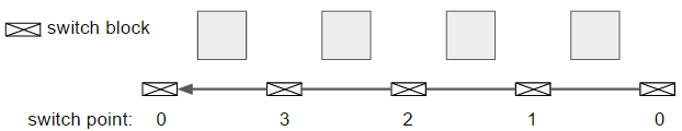
Fig. 30 Switch point diagram.
A collection of wire types and switch points defines a set of wires which will be connected to another set of wires with the specified permutation functions (the ‘sets’ of wires are defined using the <wireconn> tags).
This format allows for an abstract but very flexible way of specifying different switch block patterns.
For additional discussion on interconnect modeling see [Pet16].
The full format is documented below.
Overall Notes:
- The
<sb type="pattern">tag on a wire segment (described under<segmentlist>) is applied as a mask on the patterns created by this switch block format; anywhere along a wire’s length where a switch block has not been requested (set to 0 in this tag), no switches will be added. - You can specify multiple switchblock tags, and the switches described by the union of all those switch blocks will be created.
-
<switchblock name="string" type="string">" title="Permalink to this definition">¶ Required Attributes: - name – A unique alphanumeric string
- type –
unidirorbidir. A bidirectional switch block will implicitly mirror the specified permutation functions – e.g. if a permutation function of typelr(function used to connect wires from the left to the right side of a switch block) has been specified, a reverse permutation function of typerl(right-to-left) is automatically assumed. A unidirectional switch block makes no such implicit assumptions. The type of switch block must match the directionality of the segments defined under the<segmentlist>node.
<switchblock>is the top-level XML node used to describe connections between different segment types.
-
<switchblock_location type="string"/>" title="Permalink to this definition">¶ Required Attributes: - type –
Can be one of the following strings:
EVERYWHERE– at each switch block of the FPGAPERIMETER– at each perimeter switch block (x-directed and/or y-directed channel segments may terminate here)CORNER– only at the corner switch blocks (both x and y-directed channels terminate here)FRINGE– same as PERIMETER but excludes cornersCORE– everywhere but the perimeter
Sets the location on the FPGA where the connections described by this switch block will be instantiated.
- type –
-
<switchfuncs>¶ The switchfuncs XML node contains one or more entries that specify the permutation functions with which different switch block sides should be connected, as described below.
-
<func type="string" formula="string"/>" title="Permalink to this definition">¶ Required Attributes: - type –
Specifies which switch block sides this function should connect. With the switch block sides being left, top, right and bottom, the allowed entries are one of {
lt,lr,lb,tr,tb,tl,rb,rl,rt,bl,bt,br} whereltmeans that the specified permutation formula will be used to connect the left-top sides of the switch block.Note
In a bidirectional architecture the reverse connection is implicit.
- formula –
Specifies the mathematical permutation function that determines the pattern with which the source/destination sets of wires (defined using the <wireconn> entries) at the two switch block sides will be connected. For example,
W-tspecifies a connection where thet’th wire in the source set will connect to theW-twire in the destination set whereWis the number of wires in the destination set and the formula is implicitly treated as moduloW.Special characters that can be used in a formula are:
t– the index of a wire in the source setW– the number of wires in the destination set (which is not necessarily the total number of wires in the channel)
The operators that can be used in the formula are:
- Addition (
+) - Subtraction (
-) - Multiplication (
*) - Division (
/) - Brackets
(and)are allowed and spaces are ignored.
Defined under the
<switchfuncs>XML node, one or more<func...>entries is used to specify permutation functions that connect different sides of a switch block.- type –
-
<wireconn num_conns="expr" from_type="string, string, string, ..." to_type="string, string, string, ..." from_switchpoint="int, int, int, ..." to_switchpoint="int, int, int, ..." from_order="{fixed | shuffled}" to_order="{fixed | shuffled}"/>" title="Permalink to this definition">¶ Required Attributes: - num_conns –
Specifies how many connections should be created between the from_type/from_switchpoint set and the to_type/to_switchpoint set. The value of this parameter is an expression which is evaluated when the switch block is constructed.
The expression can be a single number or formula using the variables:
from– The number of switchblock edges equal to the ‘from’ set size.This ensures that each element in the ‘from’ set is connected to an element of the ‘to’ set. However it may leave some elements of the ‘to’ set either multiply-connected or disconnected.
to– The number of switchblock edges equal to the ‘to’ set size size.This ensures that each element of the ‘to’ set is connected to precisely one element of the ‘from’ set. However it may leave some elements of the ‘from’ set either multiply-connected or disconnected.
Examples:
min(from,to)– Creates number of switchblock edges equal to the minimum of the ‘from’ and ‘to’ set sizes.This ensures no element of the ‘from’ or ‘to’ sets is connected to multiple elements in the opposing set. However it may leave some elements in the larger set disconnected.
max(from,to)– Creates number of switchblock edges equal to the maximum of the ‘from’ and ‘to’ set sizes.This ensures all elements of the ‘from’ or ‘to’ sets are connected to at least one element in the opposing set. However some elements in the smaller set may be multiply-connected.
3*to– Creates number of switchblock edges equal to three times the ‘to’ set sizes.
- from_type – A comma-separated list segment names that defines which segment types will be a source of a connection.
The segment names specified must match the names of the segments defined under the
<segmentlist>XML node. Required if no<from>or<to>nodes are specified within the<wireconn>. - to_type – A comma-separated list of segment names that defines which segment types will be the destination of the connections specified.
Each segment name must match an entry in the
<segmentlist>XML node. Required if no<from>or<to>nodes are specified within the<wireconn>. - from_switchpoint – A comma-separated list of integers that defines which switchpoints will be a source of a connection.
Required if no
<from>or<to>nodes are specified within the<wireconn>. - to_switchpoint –
A comma-separated list of integers that defines which switchpoints will be the destination of the connections specified. Required if no
<from>or<to>nodes are specified within the<wireconn>.Note
In a unidirectional architecture wires can only be driven at their start point so
to_switchpoint="0"is the only legal specification in this case.
Optional Attributes: - from_order –
Specifies the order in which ``from_switchpoint``s are selected when creating edges.
fixed– Switchpoints are selected in the order specifiedThis is useful to specify a preference for connecting to specific switchpoints. For example,<wireconn num_conns="1*to" from_type="L16" from_switchpoint="0,12,8,4" from_order="fixed" to_type="L4" to_switchpoint="0"/>
specifies L4 wires should be connected first to L16 at switchpoint 0, then at switchpoints 12, 8, and 4. This is primarily useful when we want to ensure that some switchpoints are ‘used-up’ first.
shuffled– Switchpoints are selected in a (randomly) shuffled orderThis is useful to ensure a diverse set of switchpoints are used. For example,<wireconn num_conns="1*to" from_type="L4" from_switchpoint="0,1,2,3" from_order="shuffled" to_type="L4" to_switchpoint="0"/>
specifies L4 wires should be connected to other L4 wires at any of switchpoints 0, 1, 2, or 3. Shuffling the switchpoints is useful if one of the sets (e.g. from L4’s) is much larger than the other (e.g. to L4’s), and we wish to ensure a variety of switchpoints from the larger set are used.
Default:
shuffled - to_order –
Specifies the order in which ``to_switchpoint``s are selected when creating edges.
Note
See
from_switchpoint_orderfor value descritpions.
-
<from type="string" switchpoint="int, int, int, ..."/>" title="Permalink to this definition">¶ Required Attributes: - type – The name of a segment specified in the
<segmentlist>. - switchpoint –
A comma-separated list of integers that defines switchpoints.
Note
In a unidirectional architecture wires can only be driven at their start point so
to_switchpoint="0"is the only legal specification in this case.
Specifies a subset of source wire switchpoints.
This tag can be specified multiple times. The surrounding
<wireconn>’s source set is the union of all contained<from>tags.- type – The name of a segment specified in the
-
<to type="string" switchpoint="int, int, int, ..."/>" title="Permalink to this definition">¶ Specifies a subset of destination wire switchpoints.
This tag can be specified multiple times. The surrounding
<wireconn>’s destination set is the union of all contained<to>tags.See also
<from>for attribute descriptions.
As an example, consider the following
<wireconn>specification:<wireconn num_conns_type="to"/> <from type="L4" switchpoint="0,1,2,3"/> <from type="L16" switchpoint="0,4,8,12"/> <to type="L4" switchpoint="0/> </wireconn>
This specifies that the ‘from’ set is the union of L4 switchpoints 0, 1, 2 and 3; and L16 switchpoints 0, 4, 8 and 12. The ‘to’ set is all L4 switchpoint 0’s. Note that since different switchpoints are selected from different segment types it is not possible to specify this without using
<from>sub-tags.- num_conns –
Architecture metadata
Architecture metadata enables tagging of architecture or routing graph information that exists outside of the normal VPR flow (e.g. pack, place, route, etc). For example this could be used to enable bitstream generation by tagging routing edges and pb_type features.
The metadata will not be used by the vpr executable, but can be leveraged by new tools using the libvpr library. These new tools can access the metadata on the various VPR internal data structures.
To enable tagging of architecture structures with metadata, the <metadata>
tag can be inserted under the following XML tags:
<pb_type>- Any tag under
<interconnect>(<direct>,<mux>, etc). <mode>- Any grid location type (
<perimeter>,<fill>,<corners>,<single>,<col>,<row>,<region>)
-
<metadata>
Specifies the root of a metadata block. Can have 0 or more <meta> Children.
-
<meta name="string" >" title="Permalink to this definition">¶ Required Attributes: - name – Key name of this metadata value.
Specifies a value within a metadata block. The name is a key
for looking up the value contained within the <meta> tag. Keys can be
repeated, and will be stored in a vector in order of occurrence.
The value of the <meta> is the text in the block. Both the name and
<meta> value will be stored as a string. XML children are not supported
in the <meta> tag.
Example of a metadata block with 2 keys:
<metadata>
  <meta name="some_key">Some value</meta>
  <meta name="other key!">Other value!</meta>
</metadata>