Configurable Memory Bus-Based Tutorial
Warning
The description in this tutorial is not yet supported by CAD tools due to bus-based routing.
See also
Configurable Memory Block Example for a supported version.
Configurable memories are found in today’s commercial FPGAs for two primary reasons:
Memories are found in a variety of different applications including image processing, soft processors, etc and
Implementing memories in soft logic (LUTs and flip-flops) is very costly in terms of area.
Thus it is important for modern FPGA architects be able to describe the specific properties of the configurable memory that they want to investigate. The following is an example on how to use the language to describe a configurable memory block. First we provide a step-by-step explanation on how to construct the memory block. Afterwards, we present the complete code for the memory block.
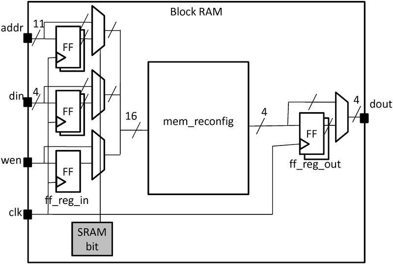
Fig. 79 Model of a configurable memory block
Fig. 79 shows an example of a single-ported memory. This memory block can support multiple different width and depth combinations (called aspect ratios). The inputs can be either registered or combinational. Similarly, the outputs can be either registered or combinational. Also, each memory configuration has groups of pins called ports that share common properties. Examples of these ports include address ports, data ports, write enable, and clock. In this example, the block memory has the following three configurations: 2048x1, 1024x2, and 512x4, which will be modeled using modes. We begin by declaring the reconfigurable block RAM along with its I/O as follows:
<pb_type name="block_RAM">
  <input name="addr" num_pins="11" equivalent="false"/>
  <input name="din" num_pins="4" equivalent="false"/>
  <input name="wen" num_pins="1" equivalent="false"/>
  <output name="dout" num_pins="4" equivalent="false"/>
  <clock name="clk" equivalent="false"/>
The input and output registers are defined as 2 sets of bypassable flip-flops at the I/Os of the block RAM.
There are a total of 16 inputs that can be registered as a bus so 16 flip-flops (for the 11 address lines, 4 data lines, and 1 write enable), named ff_reg_in, must be declared.
There are 4 output bits that can also be registered, so 4 flip-flops (named ff_reg_out) are declared:
<pb_type name="ff_reg_in" blif_model=".latch" num_pb="16" class="flipflop">
  <input name="D" num_pins="1" port_class="D"/>
  <output name="Q" num_pins="1" port_class="Q"/>
  <clock name="clk" port_class="clock"/>
</pb_type>
<pb_type name="ff_reg_out" blif_model=".latch" num_pb="4" class="flipflop">
  <input name="D" num_pins="1" port_class="D"/>
  <output name="Q" num_pins="1" port_class="Q"/>
  <clock name="clk" port_class="clock"/>
</pb_type>
Each aspect ratio of the memory is declared as a mode within the memory physical block type as shown below.
Also, observe that since memories are one of the special (common) primitives, they each have a class attribute:
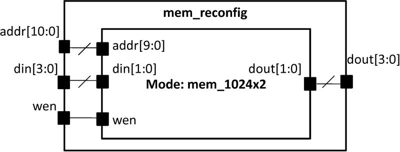
Fig. 80 Different modes of operation for the memory block.
<pb_type name="mem_reconfig" num_pb="1">
  <input name="addr" num_pins="11"/>
  <input name="din" num_pins="4"/>
  <input name="wen" num_pins="1"/>
  <output name="dout" num_pins="4"/>

  <!-- Declare a 512x4 memory type -->
  <mode name="mem_512x4_mode">
    <!-- Follows the same pattern as the 1024x2 memory type declared below -->
  </mode>

  <!-- Declare a 1024x2 memory type -->
  <mode name="mem_1024x2_mode">
    <pb_type name="mem_1024x2" blif_model=".subckt sp_mem" class="memory">
      <input name="addr" num_pins="10" port_class="address"/>
      <input name="din" num_pins="2" port_class="data_in"/>
      <input name="wen" num_pins="1" port_class="write_en"/>
      <output name="dout" num_pins="2" port_class="data_out"/>
    </pb_type>
    <interconnect>
      <direct input="mem_reconfig.addr[9:0]" output="mem_1024x2.addr"/>
      <direct input="mem_reconfig.din[1:0]" output="mem_1024x2.din"/>
      <direct input="mem_reconfig.wen" output="mem_1024x2.wen"/>
      <direct input="mem_1024x2.dout" output="mem_reconfig.dout[1:0]"/>
    </interconnect>
  </mode>

  <!-- Declare a 2048x1 memory type -->
  <mode name="mem_2048x1_mode">
    <!-- Follows the same pattern as the 1024x2 memory type declared above -->
  </mode>

</pb_type>
The top-level interconnect structure of the memory SPCB is shown in Fig. 81. The inputs of the SPCB can connect to input registers or bypass the registers and connect to the combinational memory directly. Similarly, the outputs of the combinational memory can either be registered or connect directly to the outputs. The description of the interconnect is as follows:
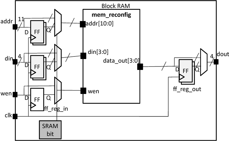
Fig. 81 Interconnect within the configurable memory block.
 1 <interconnect>
 2   <direct input="{block_RAM.wen block_RAM.din block_RAM.addr}" output="ff_reg_in[15:0].D"/>
 3   <direct input="mem_reconfig.dout" output="ff_reg_out[3:0].D"/>
 4   <mux input="mem_reconfig.dout ff_reg_out[3:0].Q" output="block_RAM.dout"/>
 5   <mux input="{block_RAM.wen block_RAM.din[3:0] block_RAM.addr[10:0]} ff_reg_in[15:0].Q"
 6        output="{mem_reconfig.wen mem_reconfig.din mem_reconfig.addr}"/>
 7   <complete input="block_RAM.clk" output="ff_reg_in[15:0].clk"/>
 8   <complete input="block_RAM.clk" output="ff_reg_out[3:0].clk"/>
 9 </interconnect>
10</pb_type>
The interconnect for the bypassable registers is complex and so we provide a more detailed explanation.
First, consider the input registers.
Line 2 shows that the SPCB inputs drive the input flip-flops using direct wired connections.
Then, in line 5, the combinational configurable memory inputs {mem_reconfig.wen mem_reconfig.din mem_reconfig.addr} either come from the flip-flops ff_reg_in[15:0].Q or from the SPCB inputs {block_RAM.wen block_RAM.din[3:0] block_RAM.addr[10:0]} through a 16-bit 2-to-1 bus-based mux.
Thus completing the bypassable input register interconnect.
A similar scheme is used at the outputs to ensure that either all outputs are registered or none at all.
Finally, we model the relationship of the memory block with the general FPGA fabric.
The ratio of tracks that a particular input/output pin of the CLB connects to is defined by fc_in/fc_out.
The pinlocations describes which side of the logic block pins reside on where the pattern spread describes evenly spreading out the pins on all sides of the CLB in a round-robin fashion.
<!-- Describe complex block relation with FPGA -->

<fc_in type="frac">0.150000</fc_in>
<fc_out type="frac">0.125000</fc_out>

<pinlocations pattern="spread"/>
Configurable Memory Bus-Based Complete Example
<pb_type name="block_RAM">
  <input name="addr" num_pins="11" equivalent="false"/>
  <input name="din" num_pins="4" equivalent="false"/>
  <input name="wen" num_pins="1" equivalent="false"/>
  <output name="dout" num_pins="4" equivalent="false"/>
  <clock name="clk" equivalent="false"/>
  <pb_type name="ff_reg_in" blif_model=".latch" num_pb="16" class="flipflop">
    <input name="D" num_pins="1" port_class="D"/>
    <output name="Q" num_pins="1" port_class="Q"/>
    <clock name="clk" port_class="clock"/>
  </pb_type>
  <pb_type name="ff_reg_out" blif_model=".latch" num_pb="4" class="flipflop">
    <input name="D" num_pins="1" port_class="D"/>
    <output name="Q" num_pins="1" port_class="Q"/>
    <clock name="clk" port_class="clock"/>
  </pb_type>

  <pb_type name="mem_reconfig" num_pb="1">
    <input name="addr" num_pins="11"/>
    <input name="din" num_pins="4"/>
    <input name="wen" num_pins="1"/>
    <output name="dout" num_pins="4"/>

    <!-- Declare a 2048x1 memory type -->
    <mode name="mem_2048x1_mode">
      <pb_type name="mem_2048x1" blif_model=".subckt sp_mem" class="memory">
        <input name="addr" num_pins="11" port_class="address"/>
        <input name="din" num_pins="1" port_class="data_in"/>
        <input name="wen" num_pins="1" port_class="write_en"/>
        <output name="dout" num_pins="1" port_class="data_out"/>
      </pb_type>
      <interconnect>
        <direct input="mem_reconfig.addr[10:0]" output="mem_2048x1.addr"/>
        <direct input="mem_reconfig.din[0]" output="mem_2048x1.din"/>
        <direct input="mem_reconfig.wen" output="mem_2048x1.wen"/>
        <direct input="mem_2048x1.dout" output="mem_reconfig.dout[0]"/>
      </interconnect>
    </mode>

    <!-- Declare a 1024x2 memory type -->
    <mode name="mem_1024x2_mode">
      <pb_type name="mem_1024x2" blif_model=".subckt sp_mem" class="memory">
        <input name="addr" num_pins="10" port_class="address"/>
        <input name="din" num_pins="2" port_class="data_in"/>
        <input name="wen" num_pins="1" port_class="write_en"/>
        <output name="dout" num_pins="2" port_class="data_out"/>
      </pb_type>
      <interconnect>
        <direct input="mem_reconfig.addr[9:0]" output="mem_1024x2.addr"/>
        <direct input="mem_reconfig.din[1:0]" output="mem_1024x2.din"/>
        <direct input="mem_reconfig.wen" output="mem_1024x2.wen"/>
        <direct input="mem_1024x2.dout" output="mem_reconfig.dout[1:0]"/>
      </interconnect>
    </mode>

    <!-- Declare a 512x4 memory type -->
    <mode name="mem_512x4_mode">
      <pb_type name="mem_512x4" blif_model=".subckt sp_mem" class="memory">
        <input name="addr" num_pins="9" port_class="address"/>
        <input name="din" num_pins="4" port_class="data_in"/>
        <input name="wen" num_pins="1" port_class="write_en"/>
        <output name="dout" num_pins="4" port_class="data_out"/>
      </pb_type>
      <interconnect>
        <direct input="mem_reconfig.addr[8:0]" output="mem_512x4.addr"/>
        <direct input="mem_reconfig.din[3:0]" output="mem_512x4.din"/>
        <direct input="mem_reconfig.wen" output="mem_512x4.wen"/>
        <direct input="mem_512x4.dout" output="mem_reconfig.dout[3:0]"/>
      </interconnect>
    </mode>
  </pb_type>

  <interconnect>
    <direct input="{block_RAM.wen block_RAM.din block_RAM.addr}" output="ff_reg_in[15:0].D"/>
    <direct input="mem_reconfig.dout" output="ff_reg_out[3:0].D"/>
    <mux input="mem_reconfig.dout ff_reg_out[3:0].Q" output="block_RAM.dout"/>
    <mux input="{block_RAM.wen block_RAM.din[3:0] block_RAM.addr[10:0]} ff_reg_in[15:0].Q"
         output="{mem_reconfig.wen mem_reconfig.din mem_reconfig.addr}"/>
    <complete input="block_RAM.clk" output="ff_reg_in[15:0].clk"/>
    <complete input="block_RAM.clk" output="ff_reg_out[3:0].clk"/>
  </interconnect>
</pb_type>

  <!-- Describe complex block relation with FPGA -->

  <fc_in type="frac">0.150000</fc_in>
  <fc_out type="frac">0.125000</fc_out>

  <pinlocations pattern="spread"/>