Multi-mode Logic Block Tutorial
This tutorial aims to introduce how to build a representative multi-mode logic block by exploiting VPR architecture description language, as well as debugging tips to guarantee each mode of a logic block is functional.
Definition
Modern FPGA logic blocks are designed to operate in various modes, so as to provide best performance for different applications. VPR offers enriched syntax to support highly flexible multi-mode logic block architecture.
Fig. 76 shows the physical implementation of a Fracturable Logic Element (FLE), which consists of a fracturable 6-input Look-Up Table (LUT), two Flip-flops (FFs) and routing multiplexers to select between combinational and sequential outputs.
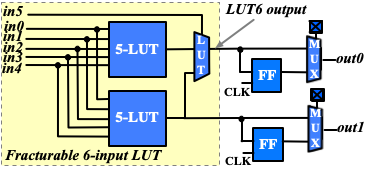
Fig. 76 Schematic of a fracturable logic element
The FLE in Fig. 76 can operate in two different modes: (a) dual 5-input LUT mode (see Fig. 77); and (b) single 6-input LUT mode (see Fig. 78). Note that each operating mode does not change the physical implementation of FLE but uses part of the programmable resources.
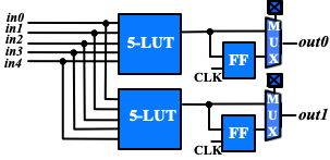
Fig. 77 Simplified organization when the FLE in Fig. 76 operates in dual 5-input LUT mode
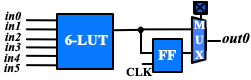
Fig. 78 Simplified organization when the FLE in Fig. 76 operates in 6-input LUT mode
Architecture Description
To accurately model the operating modes of the FLE, we will use the syntax <pb_type> and <mode> in architecture description language.
<!-- Multi-mode Fracturable Logic Element definition begin -->
<pb_type name="fle" num_pb="10">
  <input name="in" num_pins="6"/>
  <output name="out" num_pins="2"/>
  <clock name="clk" num_pins="1"/>

  <!-- Dual 5-input LUT mode definition begin -->
  <mode name="n2_lut5">
    <!-- Detailed definition of the dual 5-input LUT mode -->
  </mode>
  <!-- Dual 5-input LUT mode definition end -->

  <!-- 6-input LUT mode definition begin -->
  <mode name="n1_lut6">
    <!-- Detailed definition of the 6-input LUT mode -->
  </mode>
  <!-- 6-input LUT mode definition end -->
</pb_type>
In the above XML codes, we define a <pb_type> for the FLE by following the port organization in Fig. 76.
Under the <pb_type>, we create two modes, n2_lut5 and n1_lut6, corresponding to the two operating modes as shown in Fig. 77 and Fig. 78.
Note that we focus on operating modes here, which are sufficient to perform architecture evaluation.
Under the dual 5-input LUT mode, we can define <pb_type> and <interconnect> to model the schematic in Fig. 77.
<!-- Dual 5-input LUT mode definition begin -->
<mode name="n2_lut5">
  <pb_type name="lut5inter" num_pb="1">
    <input name="in" num_pins="5"/>
    <output name="out" num_pins="2"/>
    <clock name="clk" num_pins="1"/>
    <!-- Define two LUT5 + FF pairs (num_pb=2) corresponding to :numref:`fig_frac_lut_le_dual_lut5_mode` -->
    <pb_type name="ble5" num_pb="2">
      <input name="in" num_pins="5"/>
      <output name="out" num_pins="1"/>
      <clock name="clk" num_pins="1"/>
      <!-- Define the LUT -->
      <pb_type name="lut5" blif_model=".names" num_pb="1" class="lut">
        <input name="in" num_pins="5" port_class="lut_in"/>
        <output name="out" num_pins="1" port_class="lut_out"/>
        <!-- LUT timing using delay matrix -->
        <!-- These are the physical delay inputs on a Stratix IV LUT but because VPR cannot do LUT rebalancing,
                   we instead take the average of these numbers to get more stable results
              82e-12
              173e-12
              261e-12
              263e-12
              398e-12
              -->
        <delay_matrix type="max" in_port="lut5.in" out_port="lut5.out">
          235e-12
          235e-12
          235e-12
          235e-12
          235e-12
        </delay_matrix>
      </pb_type>
      <!-- Define the flip-flop -->
      <pb_type name="ff" blif_model=".latch" num_pb="1" class="flipflop">
        <input name="D" num_pins="1" port_class="D"/>
        <output name="Q" num_pins="1" port_class="Q"/>
        <clock name="clk" num_pins="1" port_class="clock"/>
        <T_setup value="66e-12" port="ff.D" clock="clk"/>
        <T_clock_to_Q max="124e-12" port="ff.Q" clock="clk"/>
      </pb_type>
      <interconnect>
        <direct name="direct1" input="ble5.in[4:0]" output="lut5[0:0].in[4:0]"/>
        <direct name="direct2" input="lut5[0:0].out" output="ff[0:0].D">
          <!-- Advanced user option that tells CAD tool to find LUT+FF pairs in netlist -->
          <pack_pattern name="ble5" in_port="lut5[0:0].out" out_port="ff[0:0].D"/>
        </direct>
        <direct name="direct3" input="ble5.clk" output="ff[0:0].clk"/>
        <mux name="mux1" input="ff[0:0].Q lut5.out[0:0]" output="ble5.out[0:0]">
          <!-- LUT to output is faster than FF to output on a Stratix IV -->
          <delay_constant max="25e-12" in_port="lut5.out[0:0]" out_port="ble5.out[0:0]"/>
          <delay_constant max="45e-12" in_port="ff[0:0].Q" out_port="ble5.out[0:0]"/>
        </mux>
      </interconnect>
    </pb_type>
    <interconnect>
      <direct name="direct1" input="lut5inter.in" output="ble5[0:0].in"/>
      <direct name="direct2" input="lut5inter.in" output="ble5[1:1].in"/>
      <direct name="direct3" input="ble5[1:0].out" output="lut5inter.out"/>
      <complete name="complete1" input="lut5inter.clk" output="ble5[1:0].clk"/>
    </interconnect>
  </pb_type>
  <interconnect>
    <direct name="direct1" input="fle.in[4:0]" output="lut5inter.in"/>
    <direct name="direct2" input="lut5inter.out" output="fle.out"/>
    <direct name="direct3" input="fle.clk" output="lut5inter.clk"/>
  </interconnect>
</mode>
<!-- Dual 5-input LUT mode definition end -->
Under the 6-input LUT mode, we can define <pb_type> and <interconnect> to model the schematic in Fig. 78.
<!-- 6-LUT mode definition begin -->
<mode name="n1_lut6" disable_packing="false">
  <!-- Define 6-LUT mode, consisting of a LUT6 + FF pair (num_pb=1) corresponding to :numref:`fig_frac_lut_le_lut6_mode`-->
  <pb_type name="ble6" num_pb="1">
    <input name="in" num_pins="6"/>
    <output name="out" num_pins="1"/>
    <clock name="clk" num_pins="1"/>
    <!-- Define LUT -->
    <pb_type name="lut6" blif_model=".names" num_pb="1" class="lut">
      <input name="in" num_pins="6" port_class="lut_in"/>
      <output name="out" num_pins="1" port_class="lut_out"/>
      <!-- LUT timing using delay matrix -->
      <!-- These are the physical delay inputs on a Stratix IV LUT but because VPR cannot do LUT rebalancing,
               we instead take the average of these numbers to get more stable results
          82e-12
          173e-12
          261e-12
          263e-12
          398e-12
          397e-12
          -->
      <delay_matrix type="max" in_port="lut6.in" out_port="lut6.out">
        261e-12
        261e-12
        261e-12
        261e-12
        261e-12
        261e-12
      </delay_matrix>
    </pb_type>
    <!-- Define flip-flop -->
    <pb_type name="ff" blif_model=".latch" num_pb="1" class="flipflop">
      <input name="D" num_pins="1" port_class="D"/>
      <output name="Q" num_pins="1" port_class="Q"/>
      <clock name="clk" num_pins="1" port_class="clock"/>
      <T_setup value="66e-12" port="ff.D" clock="clk"/>
      <T_clock_to_Q max="124e-12" port="ff.Q" clock="clk"/>
    </pb_type>
    <interconnect>
      <direct name="direct1" input="ble6.in" output="lut6[0:0].in"/>
      <direct name="direct2" input="lut6.out" output="ff.D">
        <!-- Advanced user option that tells CAD tool to find LUT+FF pairs in netlist -->
        <pack_pattern name="ble6" in_port="lut6.out" out_port="ff.D"/>
      </direct>
      <direct name="direct3" input="ble6.clk" output="ff.clk"/>
      <mux name="mux1" input="ff.Q lut6.out" output="ble6.out">
        <!-- LUT to output is faster than FF to output on a Stratix IV -->
        <delay_constant max="25e-12" in_port="lut6.out" out_port="ble6.out"/>
        <delay_constant max="45e-12" in_port="ff.Q" out_port="ble6.out"/>
      </mux>
    </interconnect>
  </pb_type>
  <interconnect>
    <!--direct name="direct1" input="fle.in" output="ble6.in"/-->
    <direct name="direct2" input="ble6.out" output="fle.out[0:0]"/>
    <direct name="direct3" input="fle.clk" output="ble6.clk"/>
  </interconnect>
</mode>
<!-- 6-LUT mode definition end -->
Full example can be found at link.
Validation in packer
After finishing the architecture description, the next step is to validate that VPR can map logic to each operating mode.
Since VPR packer will exhaustively try each operating mode and finally map logic to one of it.
As long as there is an operating mode that is feasible for mapping, VPR will complete packing without errors.
However, this may shadow the problems for other operating modes.
It is entirely possible that an operating mode is not defined correctly and is always dropped by VPR during packing.
Therefore, it is necessary to validate the correctness of each operating mode.
To efficiently reach the goal, we will temporarily apply the syntax disable_packing to specific modes, so as to narrow down the search space.
First, we can disable the dual 5-input LUT mode for packer, by changing
<mode name="n2_lut5">
to
<mode name="n2_lut5" disable_packing="true">
As a result, VPR packer will only consider the 6-input LUT mode during packing. We can try a benchmark mult_2x2.blif by following the design flow tutorial Basic Design Flow Tutorial. If the flow-run succeed, it means that the 6-input LUT mode is being successfully used by the packer.
Then, we can enable the dual 5-input LUT mode for packer, and disable the 6-input LUT mode, by changing
<mode name="n2_lut5" disable_packing="true">

<mode name="n1_lut6">
to
<mode name="n2_lut5">

<mode name="n1_lut6" disable_packing="true">
In this case, VPR packer will consider the dual 5-input LUT mode during packing. We can again try the same benchmark mult_2x2.blif by following the design flow tutorial Basic Design Flow Tutorial. If the flow-run succeed, it means that the dual 5-input LUT mode is being successfully used by the packer.
Finally, after having validated that both operating modes are being successfully used by the packer, we can re-enable both operating modes by changing to
<mode name="n2_lut5">
<mode name="n1_lut6">
Now, VPR packer will try to choose the best operating mode to use.
Tips for Debugging
When packing fails on a multi-mode logic block, the following procedures are recommended to quickly spot the bugs.
Apply
disable_packingto all the modes, except the one you suspect to be problematic. In the example of this tutorial, you may disable the packing for moden2_lut5and focus on debugging moden1_lut6.<mode name="n2_lut5" disable_packing="true"> <mode name="n1_lut6" disable_packing="false">
Turn on verbose output of packer
--pack_verbosity(see details in Packing Options. Recommend to use a higher verbosity number than the default value, e.g., 5. Consider the example blif and architecture in this tutorial, you may executevprwithvpr k6_frac_N10_40nm.xml mult_2x2.blif --pack_verbosity 5
Packer will show detailed information about why it fails. For example:
FAILED Detailed Routing Legality
Placed atom 'p3' (.names) at clb[0][default]/fle[4][n1_lut6]/ble6[0][default]/lut6[0][lut6]/lut[0]
(921:cluster-external source (LB_SOURCE)-->1:'clb[0].I[1]') (1:'clb[0].I[1]'-->62:'fle[0].in[1]') (62:'fle[0].in[1]'-->123:'ble6[0].in[1]') (123:'ble6[0].in[1]'-->131:'lut6[0].in[1]') (131:'lut6[0].in[1]'-->138:'lut[0].in[1]') (138:'lut[0].in[1]'-->930:cluster-internal sink (LB_SINK accessible via architecture pins: clb[0]/fle[0]/ble6[0]/lut6[0]/lut[0].in[0], clb[0]/fle[0]/ble6[0]/lut6[0]/lut[0].in[1], clb[0]/fle[0]/ble6[0]/lut6[0]/lut[0].in[2], clb[0]/fle[0]/ble6[0]/lut6[0]/lut[0].in[3], clb[0]/fle[0]/ble6[0]/lut6[0]/lut[0].in[4], clb[0]/fle[0]/ble6[0]/lut6[0]/lut[0].in[5]))
Which indicates that input ports of
<pb_type name=lut6>in the moden1_lut6may be dangling, and thus leads to failures in routing stage of packing.You may modify the architecture description and re-run vpr until packing succeeds.
Move on to the next mode you will debug and repeat from the first step.
The debugging tips are not only applicable to the example showed in this tutorial but rather general to any multi-mode logic block architecture.